Arrayed fibers are a special type of fiber structure composed of multiple individual fiber bundles arranged together in an array. Each individual fiber bundle has its own transmission channel and can independently transmit optical signals.

Arrayed fibers play important roles in many applications:

Fiber Optic Sensing: Arrayed fibers can be used as building units for fiber optic sensors. By using multiple fiber bundles, it is possible to simultaneously monitor and measure physical quantities at multiple locations, such as temperature, strain, pressure, etc. Arrayed fiber sensors have the advantage of high sensitivity and multi-channel measurement.

Medical Field: Arrayed fibers find widespread use in medical imaging and diagnosis. They can be used to construct high-resolution fiber optic coherence tomography (OCT) systems and fiber optic microscopes for real-time observation and diagnosis of tissue and cellular structures.

Industrial and Scientific Applications: In industrial and scientific research fields, arrayed fibers can be used for applications such as spectroscopy analysis, laser processing, and optical measurements. Arrayed fibers with multiple channels can provide a larger sampling range and higher data processing capability.

What is biochemical analysis? 

Biochemical analysis refers to the detection method of enzymes, carbohydrates, lipids, protein and non-protein nitrogen, inorganic elements, liver function and other indicators in the body through various biochemical reactions. It is mainly used in routine testing in hospitals. 


Biochemical diagnosis developed earlier in my country and is a routine diagnostic testing item in hospitals, focusing on disease monitoring that has already occurred. 


At present, the domestic biochemical diagnostic reagent market is relatively mature, with a complete range of reagents. Domestic brands have occupied about two-thirds of the domestic biochemical diagnostic reagent market by virtue of the advantages of cost-effective products and high-quality market services. 

Fiber Optic Cable for PCR


What is an immunoassay? 

Immunoassay is a highly selective diagnostic method established by using the specific reaction between the substance to be tested and its corresponding substance. It is often detected by the immune reaction of antigen and antibody, and various carriers are used to amplify the reaction signal to enhance the detection. Sensitivity (labels include isotopes, enzymes, chemiluminescence substances), including radioimmunity, enzyme-linked immunity,  chemiluminescence, etc., mainly to test small molecular proteins, hormones, fatty acids, drugs and other substances in the body, commonly used in infectious diseases, endocrine Detection of protein targets such as diseases, tumors, pregnancy tests, blood group antigens, etc. 


At present, high-end chemiluminescence has gradually replaced ELISA as the mainstream immunodiagnostic method in my country, focusing on the monitoring of infected diseases. 


ELISA: ELISA markers are enzymes, which are often used to detect an antigen or antibody. Reagents have the characteristics of low cost and large-scale operation, and are currently the mainstream of domestic immunodiagnostic reagents. 


Chemiluminescence: Chemiluminescence reagents have high sensitivity, strong specificity, and good reproducibility. They can be used for highly automated semi-quantitative and quantitative analysis, and have fast detection time and good reproducibility. It is one of the important development directions of immunological reagents. 


Hecho specializing in design and manufacture the Fiber Optic Cable, Optical Fiber Bundle, and Fiber Optic Light Guide for Biochemical diagnostic, Immunoassay, Molecular diagnostic, and for POCT, IVD application. Hecho supply the Customized Optical Fiber Cable which can meet the differentiated needs of different customers. 

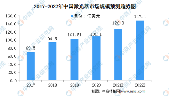
China's laser industry is developing rapidly and has obvious competitive advantages. The proportion of the global laser market has also continued to increase. In 2020, the scale of China's laser market will reach US$10.91 billion, accounting for 66.12% of the global laser market. It is expected to reach $14.74 billion in 2022.


Due to the excellent performance and strong applicability of fiber lasers, the market share has increased rapidly in the past decade. The market accounts for more than half of the market, and it has a clear leading position compared to solid-state lasers, gas lasers, and semiconductor lasers. The four major development trends are as follows:


Core components such as semiconductor laser chips are gradually being localized

Taking fiber lasers as an example, the pump source of high-power fiber lasers is the main application field of semiconductor lasers, and high-power semiconductor laser chips and modules are important components of fiber lasers. In recent years, China's fiber laser industry has been in a stage of rapid growth, and the degree of localization has increased year by year. In terms of market penetration rate, in the low-power fiber laser market, the domestic laser market share is as high as 99.01%; in the medium-power fiber laser market, the domestic laser penetration rate has maintained a level of more than 50% in recent years; the localization of high-power fiber lasers The process is also gradually advancing, reaching a penetration rate of 55.56%. However, core components such as high-power semiconductor laser chips still rely on imports. The upstream components of lasers with semiconductor laser chips as the core are gradually being localized. On the one hand, the market scale of domestic upstream components of lasers is increased. The localization of core components can improve the ability of domestic laser manufacturers to participate in international competition.


Hecho specializing in design and manufacture Customized Laser Fiber for over 18 years, which can supply the bare Fiber Optic Cables, Fiber Optic Bundles which are widely used in Laser Fiber application, such as LDI (Laser Direct Imaging), Plastic Laser Welding, and Medical application.

Recently, there has been a lot of discussion about silicon wafers. Here we analyze it from several perspectives:

Fiber Optics for Semiconductor


First of all, in terms of demand, thanks to the rise of new applications such as 5G, artificial intelligence (AI), and electric vehicles, the demand for semiconductors has increased significantly, and the shortage of chips and the expansion of foundry production have continued to benefit, and the industry market is hot. According to the statistics of the International Semiconductor Industry Association (SEMI), the global semiconductor silicon wafer shipment area will continue to grow until 2024, and show a new high performance year by year.


The huge increase in demand for silicon wafers is related to the large-scale expansion of global wafer factories in recent years. According to SEMI statistics, the number of global semiconductor factories in 2019 was 957, and it is expected to grow to 1,011 in 2022. The monthly production capacity of the factory often jumps from 30,000 to 50,000 pieces. Silicon wafers have become an indispensable strategic material, and their usage will inevitably rise in a straight line.


On the other hand, assessed from the supply side, SEMI expects global silicon wafer shipments to hit a record high year by year in the next three years. Silicon wafer manufacturers at home and abroad are unanimously optimistic about the market. After all, the foundry capacity is full, and it is undoubtedly the strongest and powerful backing for the silicon wafer industry, which is the most critical upstream raw material.


The Optical Fiber Bundles and Light Sources produced by Hecho Technology are widely used in the semiconductor industry, such as wafer inspection, cutting, Laser Direct Imaging, Automatic Optical Inspection and other fields. Different needs of different customers. 

With the gradual localization of upstream core optoelectronic components, the application cost of lasers will gradually decrease, and lasers will penetrate deeper into many industries. On the one hand, for China, laser processing also fits into the ten major application areas of China's manufacturing industry. It is expected that the application areas of laser processing will be further expanded in the future, and the market scale will be further expanded. On the other hand, with the continuous popularization and development of technologies such as unmanned driving, advanced assisted driving systems, service robots, and 3D sensing, more applications in automobiles, artificial intelligence, consumer electronics, face recognition, optical communication and defense research and many other fields. As the core device or component of the above-mentioned laser applications, semiconductor lasers will also gain space for rapid development.


Higher power, better beam quality, shorter wavelengths and faster frequencies

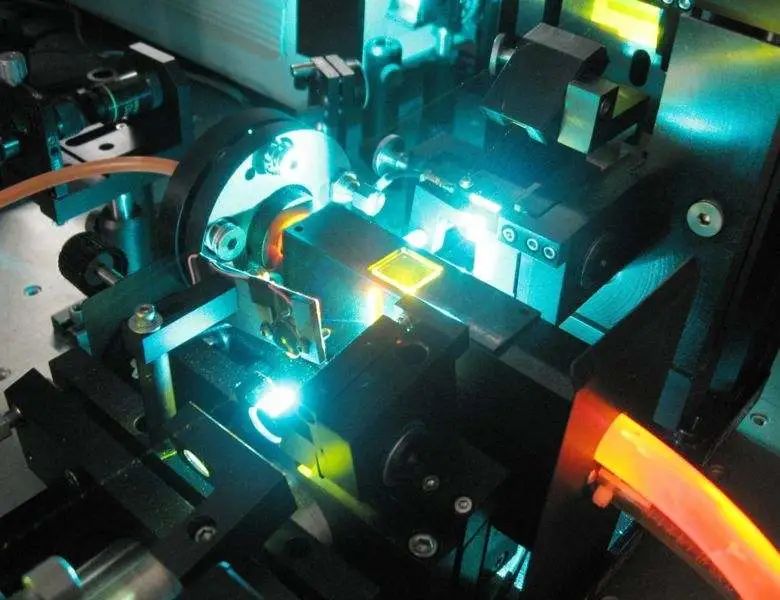
In the field of industrial lasers, fiber lasers have made tremendous progress since their inception in terms of output power, beam quality, and brightness. However, higher power can increase the processing speed, optimize the processing quality, expand the processing field to heavy industry manufacturing, and be used in cutting, welding, surface Processing, etc., the requirements for power indicators of fiber lasers continue to increase. Corresponding device manufacturers need to continuously improve the performance of core devices (such as high-power semiconductor laser chips and gain fibers), and the improvement of fiber laser power also requires advanced laser modulation technologies such as beam combining and power synthesis, which will give high-power semiconductor lasers. Chip manufacturers bring new requirements and challenges. In addition, the development of shorter wavelengths, more wavelengths, and faster (ultrafast) lasers is also an important direction, which is mainly used in integrated circuit chips, displays, consumer electronics, aerospace and other precision micromachining, as well as life sciences, medical, transmission, etc. In the fields of sense and other fields, new requirements are also put forward for semiconductor laser chips.


Demand for optoelectronic components for high-power lasers continues to grow

The R&D and industrialization of high-power fiber lasers is the result of the coordinated progress of the industry chain, which requires the support of core optoelectronic components such as pump sources, isolators, and beam combiners. The basic and key components of production, the continuous expansion of the high-power fiber laser market has also driven the market demand for upstream high-power semiconductor laser chips and other core components. At the same time, with the continuous improvement of the domestic fiber laser technology level, the realization of import substitution has become an inevitable trend, and the global laser market share will continue to increase, bringing huge opportunities for local optoelectronic component manufacturers with outstanding strength.


Nanjing Hecho Technology provides a variety of customized services for non-standard high-energy transmission optical fibers, including quartz optical fibers and glass optical fibers, which can transmit high-power lasers in the ultraviolet to infrared bands. The products are widely used in LDI Laser Direct Imaging, Plastic Laser Welding, biochemical analysis and other fields. Customized services flexibly meet the differentiated needs of different customers.
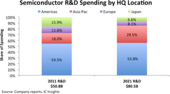
Market research firm IC Insights released an analysis of R&D trends in its latest 2022 McClean Report quarterly update, saying that about 56% of global semiconductor industry R&D spending in 2021 will come from companies headquartered in the Americas region, These companies are largely based in the United States, with a large percentage coming from Intel (19%).


As shown in the chart below, semiconductor R&D spending by companies in the Asia-Pacific region (including foundries, fabless and IDM) will exceed 29% of the global total in 2021, followed by European companies with about 8% and Japan with nearly 7%. In 2011, chip suppliers in the Americas accounted for about 55 percent of global semiconductor R&D spending, compared with 18 percent in the Asia-Pacific region (including China).


Nanjing Hecho Technology has strong optical fiber R&D and production capabilities, and can provide customized services for various Optical Fiber Bundles for different industries and usage needs to flexibly meet the differentiated needs of different customers. In addition, high-brightness LED Light Sources and Halogen Light Sources for use with optical fibers are available.
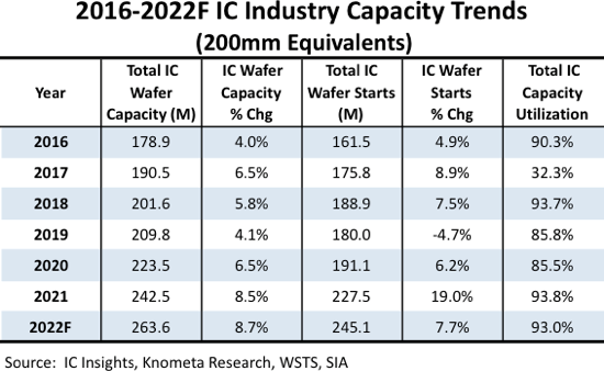
According to the latest report from IC Insights, a well-known market research institution, the total installed capacity of global semiconductors will reach 263.6 million 8-inch equivalent wafers this year, a year-on-year increase of 8.7% and a record high.


The increase in semiconductor production capacity this year is mainly due to the new large-scale memory factories of SK Hynix and Winbond, as well as the active expansion of TSMC, including the capacity growth of two advanced 5nm and 3nm processes, and the expansion of 28nm process capacity in Nanjing. TSMC is forecasting capital expenditures of more than $40 billion this year.


In the past five years, the annual growth rate of global semiconductor production capacity has increased from 4.0% in 2016 to 8.5% in 2021.


Despite inflationary pressures, ongoing supply chain issues and other economic difficulties, semiconductor demand is strong, with shipments set to grow 9.2% year over year this year. Even with 10 new fabs coming into use this year, capacity utilization could reach a high of 93% this year, slightly lower than 93.8% in 2021.


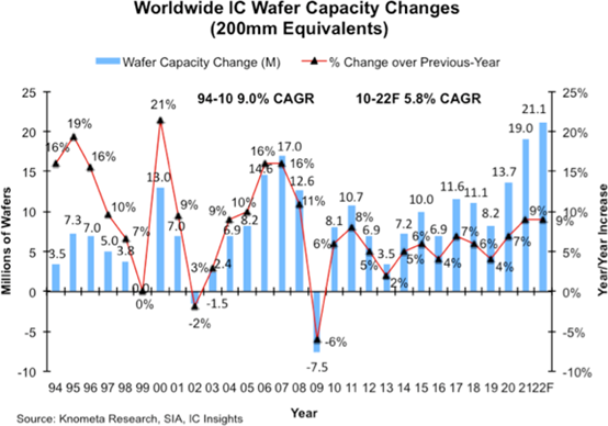
The historical statistics of IC Insights show that the growth rate of semiconductor production capacity shows a certain periodicity, with the first negative growth in 2002, and a relatively large negative growth of -6% in 2009; then it entered a boom period, which has continued to this day. The first two negative growths were the end of the dot-com bubble crisis and the global financial crisis.


Hecho Technology provides various non-standard Customized Optical Fiber and light sources, such as AOI Line Lights, LDI Laser Direct Imaging Fiber Bundle, wafer cutting, automation and other fields widely used in the semiconductor industry, to help the development of the semiconductor industry.

As China's laser industry continues to undergo the process of localization, with significant improvements in the quality of domestic products, the domestic market share of laser products, including high-power laser equipment, light sources (fiber lasers, ultrafast lasers, etc.), optical components, control systems (chips, control software, and accessories), and crystal materials, has been steadily increasing in the past two years.

According to data released by the General Administration of Customs, the total import and export value of "lasers, excluding laser diodes" in China from January to June 2023 amounted to 9.229 billion yuan, a 2.42% decrease compared to the same period last year. The import value was 6.859 billion yuan, a 12.05% decrease year-on-year, while the export value was 2.37 billion yuan, a 19.16% increase year-on-year.

Although China still relies heavily on imports for high-end equipment, the industry of laser processing machines for various materials has made significant progress in the past six years. Domestic companies have increased their exports and actively explored overseas markets, entering a favorable development stage. With policy support, important conditions have been created for the development of high-end equipment in the industry.

Source: OESHOW 


Laser direct imaging refers to Laser Direct Imaging, abbreviated as LDI, which belongs to a type of direct imaging. The light is emitted by an ultraviolet laser and is mainly used for the exposure process in the PCB manufacturing process. The imaging quality of LDI technology is clearer than that of traditional exposure technology, and it has obvious advantages in mid-to-high-end PCB manufacturing.


With the rapid progress of PCB design requirements, corresponding high-tech is required in the PCB production process (thinner materials, more complex structures, and finer graphics requirements within the range of micro-errors), traditional contact stencils Exposure and development technology can no longer meet the needs of such high-end PCB applications.


This demand has led to changes in production technology, from contact stencil exposure and development to direct laser imaging. A software-controlled laser or laser source is used to laser image a photoresist-coated PCB, or to cure and image a solder mask at the end of the PCB process.


Hecho specializes in the production of LDI optical fiber bundle, and can provide customized services for different branch numbers, lengths, and connectors according to customer needs. With strong R&D and production capabilities, it can flexibly meet the differentiated needs of different customers.
Hecho also supply customized service for AOI Line light guides, and other  Fiber Optic Bundles which for Optical Inspection equipment uses. 


LDI (Laser Direct Imaging) Industrial Chain
Upstream Midstream Downstream
Equipment Manufacturer
Motion platform and components Orbotech HDI and Standard PCB
Graphic generation module HAN'S LASER Thick copper and ceramic PCB
The light path components CFMEE Super size PCB  
The exposure light source ORC Manufacturing Others
Automatic control unit Limata 
Others Others