What is semiconductor lithography?
Fundamentals of Lithography

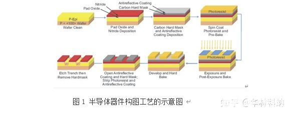
Figure 1 shows a typical lithography process for defining shallow trench isolation features. This process includes the following steps:
1. Substrate Cleaning and Preparation
2. Form a thermal oxide layer and deposit a layer of silicon nitride on a clean substrate
3. Deposit a carbon hard mask followed by a layer of anti-reflection material
4. Deposit a layer of photoresist
5. Pre-baked photoresist
6. Align the substrate/resist and reticle and expose the photoresist using UV radiation and 4x-5x imaging. Repeat steps and scan
7. Post-exposure bake
8. Develop pattern in photoresist and hard bake to remove residual solvent
9. Perform an etch to open the Dielectric Anti-Reflection Coating (DARC) and hardmask patterns, and remove the photoresist and DARC
10. Perform an etch to open trenches in the substrate and remove the hardmask
11. Clean the surface
Deep UV Lithography

DUV technology for lithography is entirely based on projection optics, as the pattern on the photomask is much larger than the final pattern formed on the photoresist. The optical system in a 193 nm lithography tool is called a catadioptric system. The term means it uses lens (refractive) and reflective (reflection) elements to direct and condition the light from the laser
Extreme UV Lithography

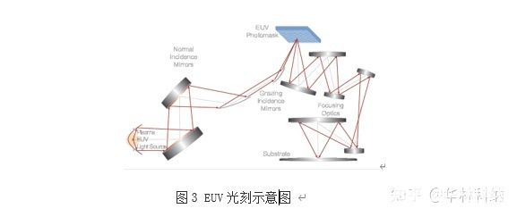
EUV lithography is being developed to meet single-exposure patterning requirements for sub-22nm feature sizes (Figure 3). What makes this technology unique is the nature of the light source. See Extreme UV Lithography for more information.
Hecho Fiber specializing in design and manufacture Fiber Optic Bundles and Fiber Optic Light Sources for over 18 years, the Fiber Products are widely used for Semiconductor filed, such as Laser Direct Imaging LDI Fiber Bundle, Fiber Optic Line Lights for AOI, and so on. OEM and ODM service is available to meet the differentiated needx of different customers.
